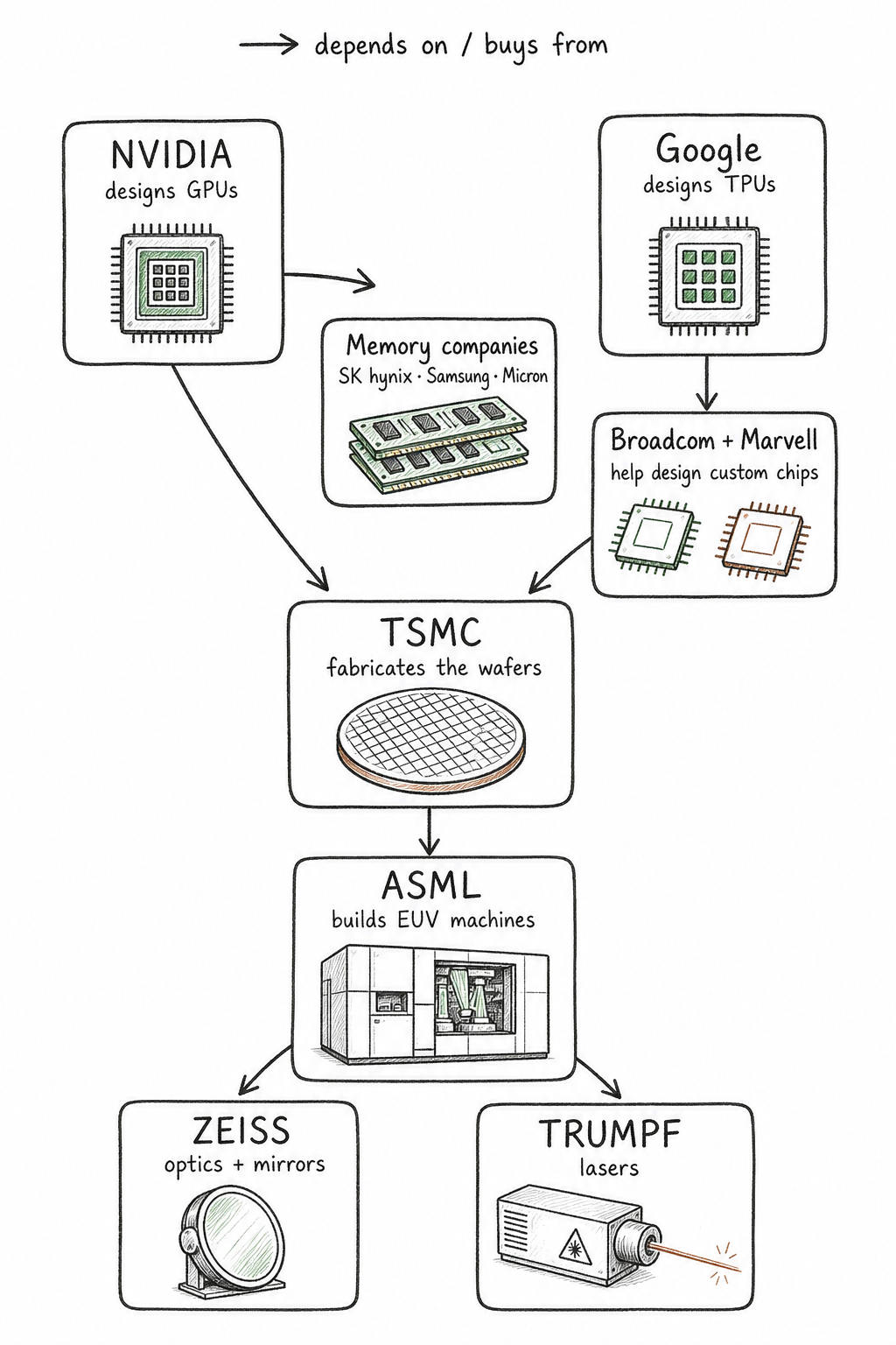
Understanding the supply chain of NVIDIA GPUs
What is an NVIDIA GPU actually made of?
The thing we call a GPU is really a package made from several parts.
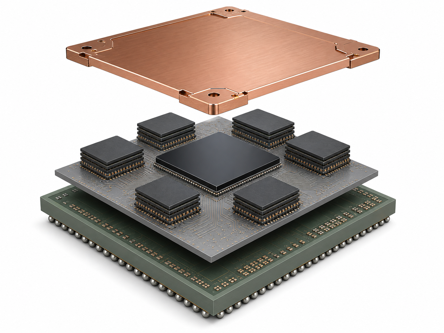
- GPU die
- Does the calculations.
- HBM
- Keeps data close to the GPU.
- Interposer
- Connects the GPU die and HBM through very dense wiring.
- Substrate
- Provides power and connects the package to the larger board.
- Cooling plate
- Sits above the package and carries heat away.
1. HBM memory
What is HBM?
HBM stands for High Bandwidth Memory. It is fast temporary memory placed beside the GPU so the GPU can get data without waiting as long.
How many companies can design it?
We cannot really know that. What we can see is that only three companies currently ship HBM at commercial scale: SK hynix, Samsung and Micron.
| Company | HBM market share Q1 2026 |
Stock return last 3 years |
|---|---|---|
| SK hynix000660 · Korea | 58% | +1,217% |
| Samsung005930 · Korea | 21% | +293% |
| MicronMU · US | 21% | +1,382% |
Market share is based on HBM revenue. Stock returns are for the whole company, not only HBM.
Sources: Counterpoint Research for Q1 2026 HBM revenue share; Yahoo Finance adjusted closes from August 21, 2023 to August 19, 2026 for SK hynix, Samsung and Micron. Package anatomy: NVIDIA and TSMC.
2. Who actually designs and makes the chips?